Details (TFC)
Methods:
(1) Hardness/adhesion
(2) Nanoindentation
(3) Plasma diagnostics and particle flux analysis
(4) Raman spectroscopy
(5) Film thickness
(6) Magnetometer (VSM) and high frequency permeameter
(7) X-ray diffraction XRD/XRR
(1) Hardness/adhesion
The film hardness can be determined by Vickers indentation with a diamond tip. The geometry of the indentation is measured by an attached optical microscope and delivers the dimensions of indentation and therefore the value of hardness.
A diamond stylus (Rockwell geometry) is scratching with linear increasing load over the coated surface. The load value at which the film begins to fail can be defined. This value is a criterion for the film adhesion. In order to optimize the substrate-film system the origin of the failure can be evaluated by the type of failure, film failure or interface failure.
Features
- Vickers hardness material independent
- Scratch test – for brittle thin film material
Limitations/constraints
- Microhardness indentation load 5 g > L > 400 g
- Critical load of failure Load 0 < L < 200g
- For hardness determination the indentation depth must be 1/10 or lower of the film thickness
Materials
Metals, alloys, ceramic, oxides, nitrides, carbides, glass
Typical structures and results
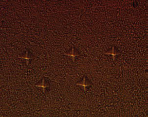
Fig. 1: Indentation for the determination of the hardness (load 50 g)
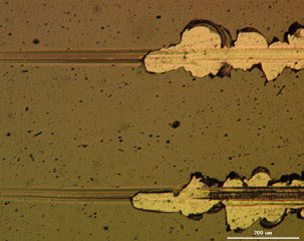
Fig. 2: Trace of the scratch test for the determination of the critical load of failure
Methods:
(1) Hardness/adhesion
(2) Nanoindentation
(3) Plasma diagnostics and particle flux analysis
(4) Raman spectroscopy
(5) Film thickness
(6) Magnetometer (VSM) and high frequency permeameter
(7) X-ray diffraction XRD/XRR
Download technology description (PDF)
(2) Nanoindentation
Nanoindentation is the most important method for the nanoscale measurement of mechanical properties (hardness, elastic modulus, fracture toughness) of surfaces, thin films and small volumes of material. A pyramidal diamond tip is pressed into the specimen as an indenter and removed again after reaching a maximum load. During this process, the load and the penetration depth of the indenter are recorded. This load/penetration depth curve represents a “finger-print” of the mechanical properties averaged over a certain volume area that increases with increasing load. The curve fitting allows the extraction of the mechanical properties.
Contact
Dr. Harald Leiste
Phone +49 721 22541-22889
Fax +49 721 608-22567
Email harald leiste ∂does-not-exist.kit edu
Institute for Applied Materials (IAM-AWP) - www.iam.kit.edu/awp/english
Features
- Force range: 10mN – 10N
- Optical system max magnification 2000x
- Min distance between indents < 250nm
- Recording of depth profiles of hardness and elastic modulus possible after special sample preparation by nanogrinding
Materials
Polymer, metal, ceramic, glass, silicon, organic
Limitations/constraints
- The surface roughness is a crucial parameter and should be < 10nm
- Indentor geometry Vickers
- Depth resolution 0.3nm
- For thin films on substrates the substrate influence on the hardness can be neglected if the indentation depth is < 1/10 of the film thickness
- For thin films on substrates there is practically no minimum indentation depth to fully exclude the substrate influence on the reduced elastic modulus
Typical structures and results
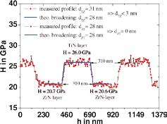
Fig. 3: Hardness depth profile of a 20-layer TiN/ZrN nanolaminated composite coating recorded at 2 mN load by small-angle cross section method (SACS)
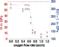
Fig. 4: Dependence of hardness and reduced elastic modulus of 100 nm thick c-BN:O films on the oxygen flow rate measured at 700 μN load
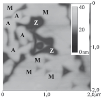
Fig. 5: AFM topography image of eutectic Al2O3-ZrO2 region in a laser-modified alumina ceramic showing nanoindents (maximum load: 1 mN; M = Al2O3 matrix, A =Al2O3 lamella, Z = ZrO2 lamella)
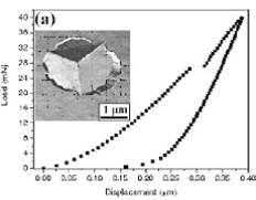
Fig. 6: Load–displacement curve and AFM image (insert) of the cracking of a TiAlN single-layered coating for the calculation of fracture toughness
Methods:
(1) Hardness/adhesion
(2) Nanoindentation
(3) Plasma diagnostics and particle flux analysis
(4) Raman spectroscopy
(5) Film thickness
(6) Magnetometer (VSM) and high frequency permeameter
(7) X-ray diffraction XRD/XRR
Download technology description (PDF)
(3) Plasma diagnostics and particle flux analysis
Low pressure plasmas can be characterized by electrical single and double probes and optical emission spectroscopy. The particle fluxes onto the substrates can be determined by Faraday cup as well as retarding field analyzer. Based on the measurements the following physical quantities are calculated: electron temperature Te, plasma density ne, ion and electron current density jion and je, plasma potential Upl, ion energy Eion, energy distribution of ions f(Eion).
Contact
Dr. Harald Leiste
Phone +49 721 22541-22889
Fax +49 721 608-22567
Email harald leiste ∂does-not-exist.kit edu
Institute for Applied Materials (IAM-AWP) - www.iam.kit.edu/awp/english
Features
- Faraday cup/retarding field analyzer: 0–1000 eV
- Single- and double probe: plane and cylindrical
- Optical emission spectrometer: 200 –800 nm
Limitations/constraints
- Height: 50 mm, diameter: 80 mm
- Temperature range: RT–200 °C
- KF40 flange utilizable
- The whole system is transportable
Typical results
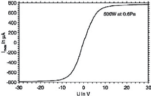
Fig. 7: Current–voltage-characteristic of a double probe measurement (r.f. magnetron argon plasma)

Fig. 8: Energy distribution of Ar-ions during film growth by magnetron sputtering
Typical setups
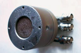
Fig. 9: Retarding field analyzer for measurement of plasma potential, ion energy and energy distribution ions
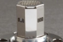
Fig. 10: Micropole mass spectrometer mounted on KF16 flange
Methods:
(1) Hardness/adhesion
(2) Nanoindentation
(3) Plasma diagnostics and particle flux analysis
(4) Raman spectroscopy
(5) Film thickness
(6) Magnetometer (VSM) and high frequency permeameter
(7) X-ray diffraction XRD/XRR
Download technology description (PDF)
(4) Raman spectroscopy
By laser excited Stokes Raman scattering the chemical bonding and microstructure of compact, powder and thin film materials are evaluated. In solid state physics, Raman spectroscopy has become an important method to investigate carbon species and a-C: metal nanocomposites. Raman spectroscopy is also suitable for the microscopic examination of minerals, polymers and ceramics, but also of cell and proteins. Recently, the Raman spectroscopy could be used for measuring concentration profiles within micro channels.
Contact
Dr. Harald Leiste
Phone +49 721 22541-22889
Fax +49 721 608-22567
Email harald leiste ∂does-not-exist.kit edu
Institute for Applied Materials (IAM-AWP) - www.iam.kit.edu/awp/english
Features
- Backscattering geometry
- Excitation with Argon-Ion-Laser (514.5 nm)
- Excitation with Helium-Cadmium-Laser (325 nm)
- Holographic grating 2400 grooves mm-1
- UV-enhanced CCD detector with thermo-electric cooling
Limitations/constraints
- Spectral resolution 1–2 cm-1
- Spectral range (Raman shift) < 200–4000 cm-1
- Spatial resolution 2 μm lateral (x 50 objective)
- Confocal mode possible
- Typical sample: flat, thin film, fine powder
Materials
Metal, ceramic, glass, silicon, polymer
Typical setup
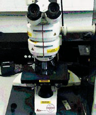
Fig. 11: Optical arrangement for Micro Raman spectroscopy
Typical results
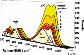
Fig. 12: Raman spectra of six samples with different Ti:C ratios deposited using -150 V substrate bias voltage
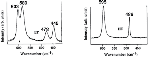
Fig. 13: Characterisation of LiCoO2 phases
Methods:
(1) Hardness/adhesion
(2) Nanoindentation
(3) Plasma diagnostics and particle flux analysis
(4) Raman spectroscopy
(5) Film thickness
(6) Magnetometer (VSM) and high frequency permeameter
(7) X-ray diffraction XRD/XRR
Download technology description (PDF)
(5) Film thickness
The film thickness can be determined by calo-test, where a spherical calotte will be polished into the surface. The sectional view diameters provide, together with the geometry of the grinding sphere, the value of the film thickness. By the use of a surface profilometer (Type Tencor P10), the roughness, waviness, step size of uncoated/coated regions and curvature of bending can be measured by the stylus method with a diamond tip.
Contact
Dr. Harald Leiste
Phone +49 721 22541-22889
Fax +49 721 608-22567
Email harald leiste ∂does-not-exist.kit edu
Institute for Applied Materials (IAM-AWP) - www.iam.kit.edu/awp/english
Features
- Calo-test is a local destructive methode
- Roughness values like Ra,Rt, Rz will be given
Limitations/constraints
- Calo-test film thickness 500 nm < t < 5 μm; min. film area 1mm
- Profilometer film thickness 20 nm < t < 5 μm; max. scan length 150 mm
- Resolution and accuracy depends on roughness
Materials
Metal, ceramic, glass, polymer
Typical results
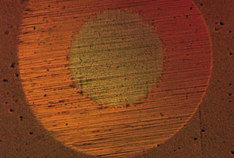
Fig. 14: A calotte polished into a coated substrate
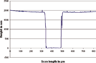
Fig. 15: Surface profile of a partial coated substrate
Methods:
(1) Hardness/adhesion
(2) Nanoindentation
(3) Plasma diagnostics and particle flux analysis
(4) Raman spectroscopy
(5) Film thickness
(6) Magnetometer (VSM) and high frequency permeameter
(7) X-ray diffraction XRD/XRR
Download technology description (PDF)
(6) Magnetometer (VSM) and high frequency permeameter
For the characterisation of ferromagnetic thin films properties especially the determination of magnetic hysteresis behaviour a vibrating sample magnetometer can be used to determine the saturation magnetisation Ms, the coercivity Hc, permeability μ and anisotropy Ha. The high frequency permeability with real and imaginary (damping) part can be determined by the use of a coplanar measuring head in a frequency range of 30 kHz < f < 6 GHz.
Contact
Dr. Harald Leiste
Phone +49 721 22541-22889
Fax +49 721 608-22567
Email harald leiste ∂does-not-exist.kit edu
Institute for Applied Materials (IAM-AWP) - www.iam.kit.edu/awp/english
Features
- Vibrating sample magnetometer for thin film samples (max field 600 mT)
- High frequency permeameter 30 kHz < f < 6 GHz
Limitations/constraints
- Vibrating sample magnetometer: Min film thickness min 50 nm
- Vibrating sample magnetometer typical sample: flat, thin film, size 5 x 5 x 0.5 mm3
- High frequency permeameter, sample size 5 x 5 x 0.3 mm3
Materials
Ferromagnetic thin films on silicon, ceramic, glass
Typical setups and results
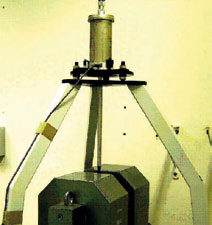
Fig. 16: Vibrating sample magnetometer (VSM)
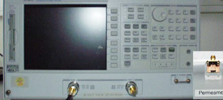
Fig. 17: The high frequency permeameter consists of a strip-line measuring head on an attached vector network analyzer
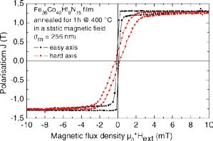
Fig. 18: Magnetic hysteresis of a thin ferromagnetic thin film with uniaxial anisotropy (easy axis of magnetisation (black) and hard axis of magnetisation (red)
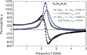
Fig. 19: Frequency dependent permeability; real part (black) and imaginary part (blue)
Methods:
(1) Hardness/adhesion
(2) Nanoindentation
(3) Plasma diagnostics and particle flux analysis
(4) Raman spectroscopy
(5) Film thickness
(6) Magnetometer (VSM) and high frequency permeameter
(7) X-ray diffraction XRD/XRR
Download technology description (PDF)
(7) X-ray diffraction XRD/XRR
By means of X-ray radiation (Cu-cathode) the microstructure of powder, compact and thin film material can be measured and evaluated. Different geometries, and circle movements (Bragg-Brentano-geometry, GID, texture, X-ray reflectivity) can be realized. It can be decided if the material is amorphous or crystalline, and the lattice parameters can be determined from the line positions.
Contact
Dr. Harald Leiste
Phone +49 721 22541-22889
Fax +49 721 608-22567
Email harald leiste ∂does-not-exist.kit edu
Institute for Applied Materials (IAM-AWP) - www.iam.kit.edu/awp/english
Features
- Bragg-Brentano
- Texture
- XRR-characterisation
- RSM
- Cu-X-ray tube
- Optional monochromator
- Compact material, thin films, powder samples
Limitations/constraints
- Resolution 1/10000°
- Max. sample load 5 kg
- Min. beam Ø 2mm
- XRR typical sample: flat, thin film, size 20x20x1mm3
- Min sample size 5x5mm2
- Max sample size Ø 150mm x 20mm
Materials
Metal, ceramic, bulk, powder, thin films
Typical setup
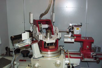
Fig. 20: 4 circle goniometer for XRD characterization (Seifert 3003 HR)
Typical results
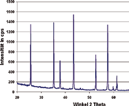
Fig. 21: Bragg-Brentano diagram of Al2O3-sample
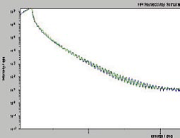
Fig. 22: XRR-diagram of a thin film for density determination
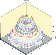
Fig. 23: Texture diagram of TiN thin film

