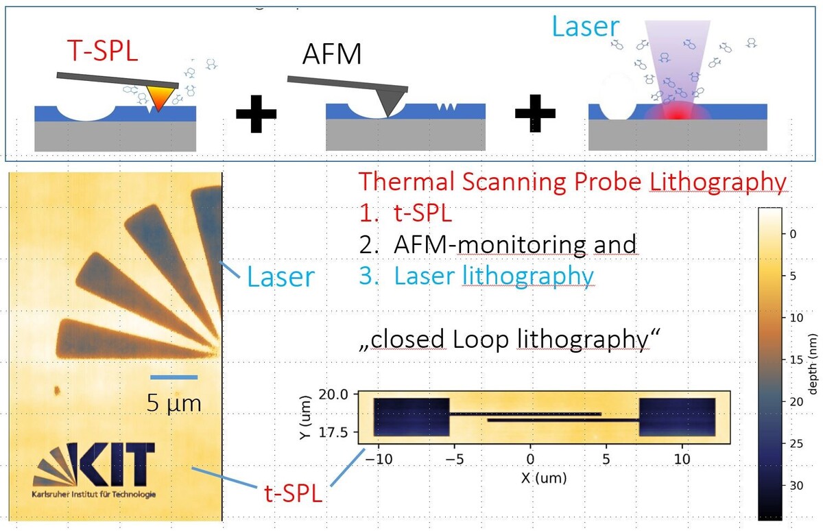
Thermal Scanning Probe Lithography (t-SPL)
t-SPL Technology: High-Resolution Scanning Probe Nanolithography, Direct Writing
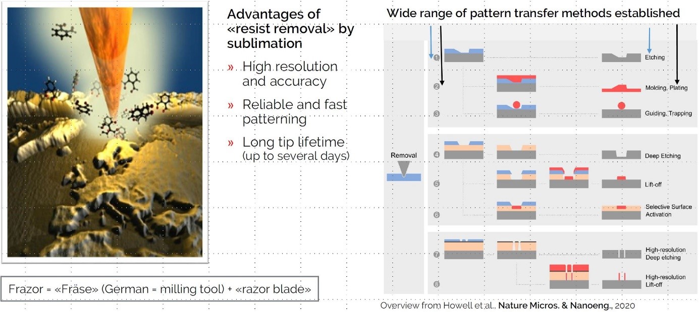
The heated AFM probe (up to 1100°C) directly evaporates a thermally sensitive resist without requiring any development or proximity correction. This allows for the generation of complex greyscale shapes with a vertical resolution of 2 nm. The smallest feature size is 15 nm, and periodic lines and spaces can be achieved with a half-pitch of 25 nm. The write speed is 1 mm/s, and the sample dimensions can be up to 100 mm x 100 mm with a height of up to 15 mm.
In-situ Topographic AFM-Imaging
The same tip is used for both lithography and imaging. It is heated for lithography and cooled down for imaging the topography. Deviations from the target design are detected and used as input for immediate adjustments of the patterning parameters.
Integrated Micro-Lithography with Direct Laser Sublimation and In-situ AFM-Monitoring
The same resist layer, platform, and software are used for laser writing, combined with in-situ AFM-imaging. A focused 405 nm laser beam with a maximum output power of 110 mW on the sample is used for the direct sublimation of resists like PPA. A feature size of 600 nm is specified, with a stitching accuracy of 300 nm and a typical writing speed of 5 mm/s.
Details (t-SPL)
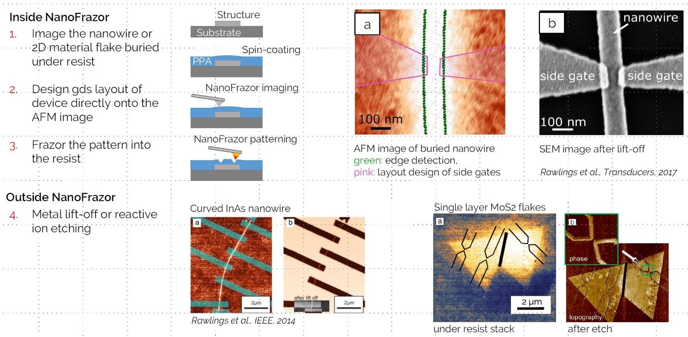
Marker-less Overlay
- t-SPL does not require sample alignment using artificial marker structures
- Randomly assembled nanowires or 2D material flakes down to the monolayer thickness (< 1 nm Topography) can be detected, even when they are buried under the resist layers.
No damage to delicate materials
- No charged particles beam
Negligible heating of the underlying substrate - Hence better device performance with sensitive materials
Thermal nano-scale experiments
- Allows for material conversion at the nanoscale (phase change materials, chemical reactions,…)
Layout design and software
- Layout design in the formats of GDSII, JPG, PNG, BMP, TIFF can be imported to the operating software of the system
- Up to 256 depth levels can be defined for greyscale lithography
Materials
- A wide range of substrates can be processed, like glass, silicon, plastics or metal-organics.
- Metallic, Conductive or Isolating. Discuss your particular wish with the KNMFi technology experts.
Limitations/constraints
- Sample size < 10 x10 cm, (height < 3 cm)
Typical structures and designs (t-SPL)
Local sublimation of the resist, without irradiation with electrons or ions or UV-light with minimal thermal heating of the substrate
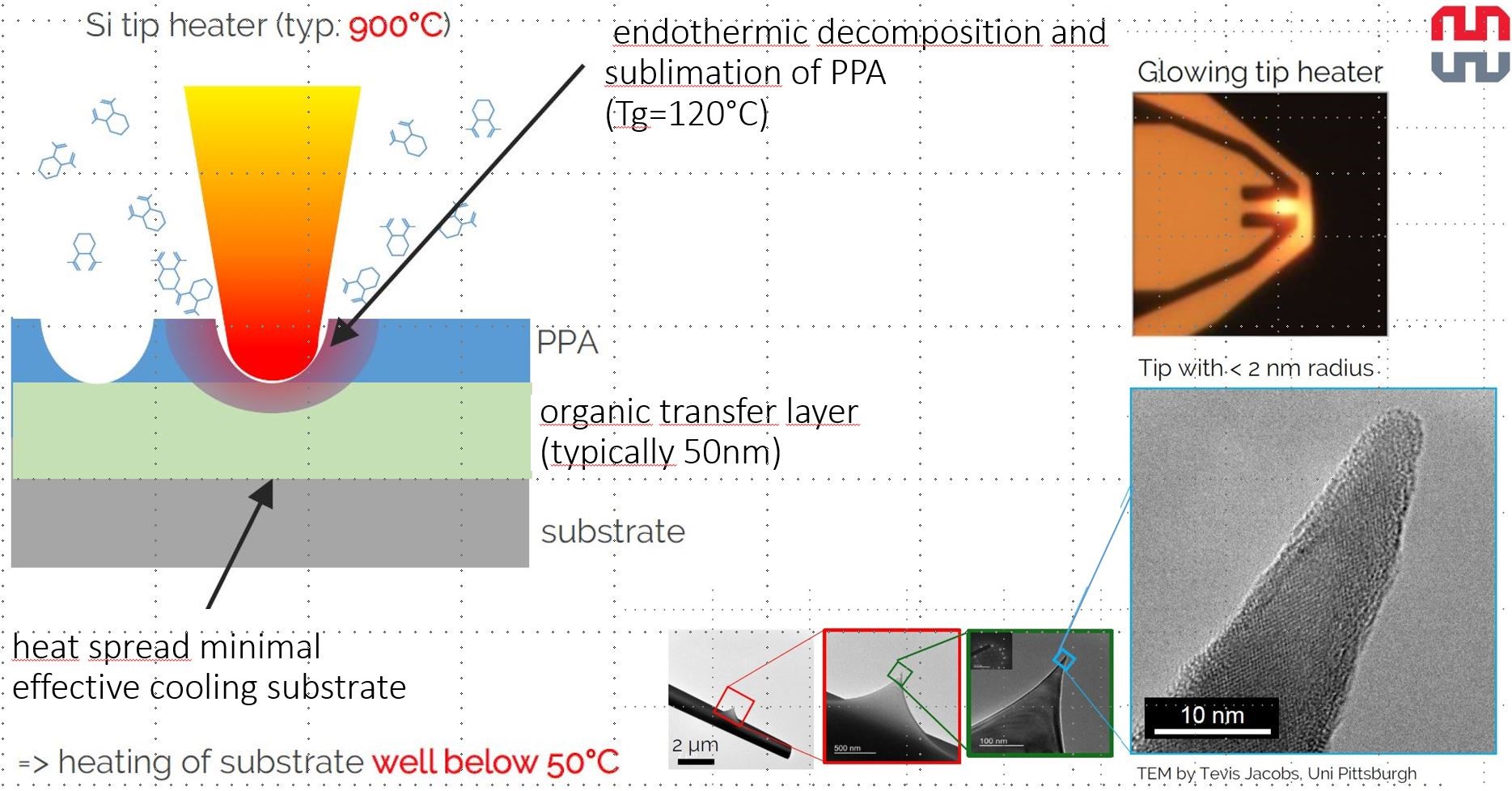
Resist removal with a heated nano-tip by sublimation [1]
Nano fabrication for contacting nano objects as nanowires or 2D-material [1]
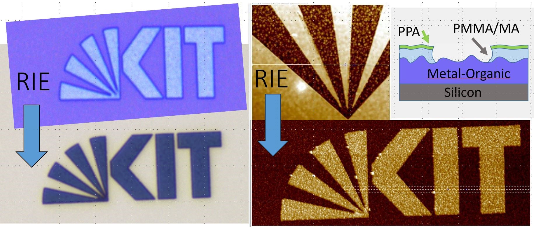
First results of a relatively rough, t-SPL-patterned metal-organic layer
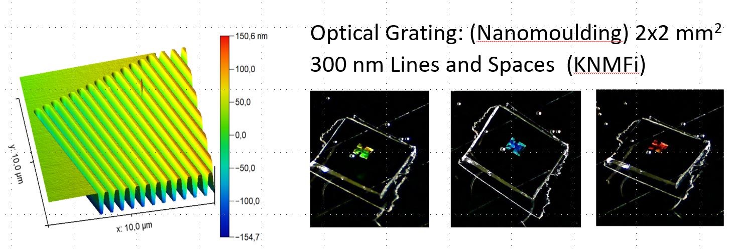
2x2 mm2 (gratings 300 nm lines and spaces), structured with t-SPL. Pattern transfer with RIE in Silicon and nano-moulding in transparent thermoplastic materials (see interference coulours)
References (t-SPL)
- Howell S.T., Grushina A., Holzner F. and Brugger J.
Thermal scanning probe lithography - a review
Microsystems & Nanoengineering (2020) 6:21
https://doi.org/10.1038/s41378-019-0124-8


